Guitar Distortion Effect Stomp box
Contents
- Overview
- Demo
- The Build Progress
- Overall Design
- Power Supply
- Input Buffer Stage
- Input Buffer Bypass
- Distortion and Diode Clipping
- Tone Control
- Output Booster Stage
- Distortion Bypass
- Printed Circuit Board
- Enclosure
- Bill of Materials
Overview
FrankenStomp is my first attempt at a guitar distortion effect stomp box. Building this was a pretty good excuse to pick up my guitar again after having not played for a while.
It’s all analog, so no fancy digital signal processing here. The design takes inspiration from other effects, like the clipping circuit topology from the Boss DS-1 pedal and the output buffer and level control from the Big Muff Pi. Combined with some random stuff from the parts bin, it’s a Frankenstein mashup of a project, so FrankenStomp seems like a good name.
I felt I learned a lot by studying other effect designs to get some basic ideas of what they do to the guitar signal. Despite still not really knowing what I’m doing when it comes to audio, I’m pretty happy with the results.
This page is not meant to be a complete tutorial on how to build it. The intent is to document the key parts of the project.
Demo
The Build Progress
Overall Design
A distortion effect includes a few main functions:
- Signal buffering, prevents the circuit from interfering with other attached effects or tone loss
- Signal distortion, or clipping (the main thing!)
- Guitar signal amplification
- Tone and level control
- Removing unwanted frequencies/signals (low and high pass filtering)
A unique (stupid?) aspect includes the use of two, true bypass switches. The first bypass is for enabling and disabling the input buffer. The second is for the distortion effect itself, which is usually what a bypass is for. When trying out the input buffer, I couldn’t decide if I liked it, but it gave the sound interesting characteristics when combined with the distortion and gave a “crisp” sound when the distortion was bypassed and the guitar’s tone control set all the way up. So if you’re undecided about something in the moment, you might as well add a way to switch it on and off.
The bypass is “true” in the sense that the switches allow the pure guitar signal to completely bypass the buffer and distortion effect. When both bypasses are set, it’s a direct connection between the guitar and the amp and no power to the stomp box is needed.
These switches have 9 pins each and are a pain to wire up. No wonder you don’t see this on mass-produced effects.
I used open source KiCad to design this. Click on the schematic below to get a full-sized version.
Power Supply

The box runs on 9 volts, which can be supplied either from a 9v wall wart plugged into J3, or a typical 9v battery (BT1). Switch it on with SW3. Any single-pole, single-throw (SPST) switch will do. I used a rocker switch out of an old ice cream maker.
Plugging the wall wart into J3 disconnects the battery so it goes off of wall power instead. D6 is a LED power indicator.
The power supply circuit itself took some inspiration from the Boss DS-1 in that it supplies the 9v to most of the circuit, while using a voltage divider (R16 and R17) to provide a 4.5v bias voltage to the input buffer, and includes a reverse voltage protection diode (D4). D4 prevents damage if you plug the power in the wrong way. C11 and C13 provide some voltage smoothing for the 4.5v bias.
Input Buffer Stage

Usually the point of an input buffer on a guitar effect is to preserve tonal qualities of the input signal by providing high input impedance. I’m using an op-amp topology inspired by the guide on buffers at muzique.com. The NE5534N is a low-noise op-amp I had in the parts bin, and it gives the tone some interesting “brightening” characteristics when enabled via the the first bypass switch. Check the demo video to hear the effect.
Input Buffer Bypass

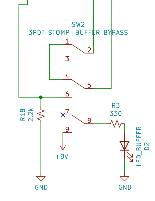
FrankenStomp uses two 3PDT switches to allow independent bypassing of the input buffer stage and distortion stages (see below). These are 9-terminal switches and are a pain to wire up. But done correctly, you can get a direct connection between the guitar output and amp with both bypasses enabled so it doesn’t affect the signal. In fact, you can power off FrankenStomp entirely and still get a signal to the amp since both switches enabled bypass all circuit stages.
The input buffer bypass has a bleed-down resistor (R18) to eliminate the “DC thump” or popping sound when switching this stage.
An oscilloscope showed a voltage spike during switching, which could reach as high as 9v, which is the power supply. My guess as to the cause would be a charge built up in C2 on the output of the input buffer. Aside from the placement, C2 is the largest capacitor in the audio stages of this circuit, so it’s liable to build up a big charge. Safely bleeding this off to ground through a resistor seemed like the way to go.
But how do we size R18?
We can use the bleed resistor formula, and the handy calculator at Digikey:
Rb is the value of the bleed resistor in ohms, which is what we need to calculate.
τ is the time to discharge the capacitor. We’ll choose .1 seconds, or 100 milliseconds. Seems fast enough for a discharge.
C is our capacitor value, which is 10uf.
Vt is a voltage up to what we can discharge. Let’s say 50 millivolts, or 0.05 volts, since the guitar voltage signals operate in this range.
Vi is the initial voltage, which is from the 9v power supply.
Rb works out to about 1925 ohms. So a 2.2K resistor from the parts bin works here.
Just for the hell of it, I tried other values. 10K ohm also keeps the circuit quiet, but the oscilloscope shows a voltage jump that’s higher than 50 millivolts, something like 2-3 volts. A 100K resistor is clearly too large, giving too slow of a discharge and not helping with the thump sound.
LED D2 indicates whether the input bypass is enabled.
Distortion and Diode Clipping

This stage does the distortion heavy lifting. D3 and D5 Schottky diodes (1N6263) provide hard clipping on the output of the LF351N op-amp. Their job is to “chop off” the peaks and lows of the audio wave form, which creates distortion. The R5 potentiometer controls the gain out of the op-amp. The topology here is inspired by the Boss DS-1 distortion pedal described on Electrosmash.
C3 and R4 form a high pass filter with a cutoff frequency of around 23 Hz to remove unwanted low end. Potentiometer POT1_DIST1 controls the gain. The demo video shows the effect.
Tone Control

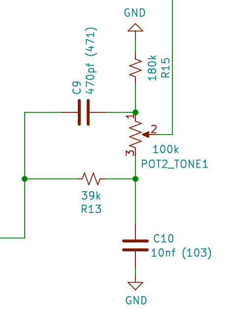
The tone control of FrankStomp is inspired by the Big Muff Pi stage described on Electrosmash. High-pass and low-pass filters comprise the tone control with potentiometer POT2_TONE1. The low-pass filter with R13 and and C10 give a low cutoff frequency of about 408 h5 Hz and the high-pass filter with C9 and R1 give a high cutoff of about 1.881 Khz. The potentiometer adjusts tone between those two points.
Output Booster Stage

The distortion circuit caused some signal loss, so some output boosting was needed to compensate. Without some boosting, the distorted sound outputs at a lower volume than the clean one. To compensate, while making this all play nice with the amp connected to the output, a common-emitter amplifier was used to boost the volume in a similar to the Big Muff Pi output booster. The Q1 transistor does the amplifying. The volume at the booster output is controlled using POT2_DIST_VOL1. Adjusting this allows you to set the volume of the distortion to the same volume as the clean sound when the bypass is enabled.
The voltage divider created by R7 and R8 provide the voltage bias at the base of Q1.
Placed after the distortion bypass switch SW1 (but still considered part of this output stage), R14 and C12 form a low pass filter that cleans up some hum, with a cutoff of about 2.2 KHz.
Distortion Bypass

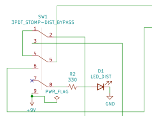
The distortion bypass wiring is exactly the same as the input buffer, except there’s no bleed-down resistor. LED D1 indicates whether the distortion is enabled (i.e. not bypassed).
This switch also bypasses the tone and output buffer stages.
Printed Circuit Board (PCB)

Like the schematic, the PCB was designed using KiCad and was made by OshPark. The audio quality was better on the PCB compared to the breadboard, due to better connections. The various headers make connecting the audio jacks, switches and knobs easier. The op amp ICs are using DIP sockets for easy chip replacement. You wouldn’t add all of these extra parts on a mass-produced item, but it’s a one-off project and being able to change and repair things easily was more important here than having a perfectly optimized bill of materials.
Enclosure
I suck at making enclosures. You’d think this would be the easiest part, but not for me. However, there’s no escaping this if things I build are to be actually usable. Do I get a pre-made project box that won’t fit right, or spend the time making my own?
I ended up 3d-printing an enclosure and related parts out of the transparent PETG that was already loaded into my Ender 3 Pro printer. The box came out a translucent white, which lets LEDs shine through the box for a nice effect. Not having to drill holes through the box was also convenient.

The lettering is a raised part of of the print, and was colored with a green Sharpie marker. Ink bleeds into the layers on the side wall lettering, but I like the effect.
Bill of Materials
| Reference | Qnty | Value | Description |
|---|---|---|---|
| BT1 | 1 | 9V BAT | 9v Battery |
| C1, C3, C5, C7, C8 | 5 | 100nf (104) | Unpolarized capacitor |
| C2 | 1 | 10uf | Polarized Capacitor |
| C4, C9 | 2 | 470pf (471) | Unpolarized capacitor |
| C6 | 1 | 100p (101) | Unpolarized capacitor |
| C10 | 1 | 10nf (103) | Unpolarized capacitor |
| C11 | 1 | 100uf | Polarized Capacitor |
| C12 | 1 | 22nf (2A223J) | Unpolarized capacitor |
| C13 | 1 | 47uf | Polarized Capacitor |
| D1 | 1 | LED_DIST | Red Light emitting diode |
| D2 | 1 | LED_BUFFER | Yellow Light emitting diode |
| D3, D5 | 2 | 1N6263 | Schottky clipping diodes |
| D4 | 1 | 1N4001 | 50V 1A General Purpose Rectifier Diode, DO-41 for reverse polarity protection |
| D6 | 1 | LED_PWR | Green Light emitting diode |
| J1 | 1 | Input | Audio Jack, 2 Poles (Mono / TS) |
| J2 | 1 | Output | Audio Jack, 2 Poles (Mono / TS) |
| J3 | 1 | BARREL_JACK_SW | DC Barrel Jack with an internal switch |
| POT1_DIST1 | 1 | 500k | Gain Potentiometer (Linear) |
| POT2_DIST_VOL1 | 1 | 100k | Level Potentiometer (Linear) |
| POT2_TONE1 | 1 | 100k | Tone Potentiometer (Linear) |
| Q1 | 1 | 2N5809 | 0.2A Ic, 40V Vce, Small Signal NPN Transistor, TO-92 |
| R1 | 1 | 1m | Resistor, small US symbol |
| R2, R3, R12 | 3 | 330 | Resistor, small US symbol |
| R4 | 1 | 68k | Resistor, small US symbol |
| R5 | 1 | 4.7k | Resistor, small US symbol |
| R6, R8 | 2 | 100k | Resistor, small US symbol |
| R7 | 1 | 470k | Resistor, small US symbol |
| R9, R16, R17 | 3 | 10k | Resistor, small US symbol |
| R10, R11, R18 | 3 | 2.2k | Resistor, small US symbol |
| R13 | 1 | 39k | Resistor, small US symbol |
| R14 | 1 | 3.3k | Resistor, small US symbol |
| R15 | 1 | 180k | Resistor, small US symbol |
| SW1 | 1 | 3PDT_STOMP-DIST_BYPASS | Distortion bypass Stomp Switch |
| SW2 | 1 | 3PDT_STOMP-BUFFER_BYPASS | Input buffer bypass Stomp Switch |
| SW3 | 1 | SW_PWR | Power switch |
| U1 | 1 | NE5534N | Single Low-Noise Operational Amplifiers, DIP-8/SOIC-8 |
| U2 | 1 | LF351N | Wide bandwidth single JFET operational amplifier, DIP-8 |


